1. Zener Diode Tester Circuit
Using a single 555 Timer IC and a small transformer to generate a high voltage, this circuit will test zener diodes of voltage ratings up to 50VDC. The 555 timer is used in the astable mode, the output at pin3 drives a small audio transformer such as the LT700. This has a primary impedance of 1K and a secondary impedance of 8 ohms. Used in reverse the unloaded ac voltage is around 120volts ac. This is rectified by the 1N4004 diode and smoothed by the 2.2u capacitor which MUST be rated at 150 VDC. The zener under test is measured with a multimeter set to DC volts as shown. The load current switch enables the zener to be tested at 1 or 2mA DC. The rectified DC load, but a good zener should maintain the reading on the volt meter.
2. Infra Red Remote Control Tester Circuit
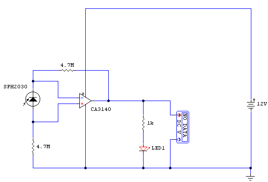
This circuit is the result of Andy Collinson research. He has used a photodiode, SFH2030 as an infra red sensor. A MOSFET opamp, CA3140 is used in the differential mode to amplify the pulses of current from the photodiode. LED1 is an ordinary coloured led which will light when IR radiation is being received. The output of the opamp, pin 6 may be connected to a multimeter set to read DC volts. Infra red remote control strengths can be compared by the meter reading, the higher the reading, the stronger the infra red light. He aimed different remote control at the sensor from about 1 meter away when comparing results. For every microamp of current through the photodiode, about 1 volt is produced at the output. A 741 or LF351 will not work in this circuit. Although he has used a 12 volt power supply, a 9 volt battery will also work here.
3. Electromagnetic Field Probe with Meter
Notes:Using a single 555 Timer IC and a small transformer to generate a high voltage, this circuit will test zener diodes of voltage ratings up to 50VDC. The 555 timer is used in the astable mode, the output at pin3 drives a small audio transformer such as the LT700. This has a primary impedance of 1K and a secondary impedance of 8 ohms. Used in reverse the unloaded ac voltage is around 120volts ac. This is rectified by the 1N4004 diode and smoothed by the 2.2u capacitor which MUST be rated at 150 VDC. The zener under test is measured with a multimeter set to DC volts as shown. The load current switch enables the zener to be tested at 1 or 2mA DC. The rectified DC load, but a good zener should maintain the reading on the volt meter.
4. Simple Square Wave Oscillator
Using two gates from a CMOS 4011 NAND chip, a simple Squarewave oscillator can br made. Alternatively a CMOS 4001 chip can also be used, or a TTL equivalent. In this circuit the mark space ratio can also be independently controlled by varying the value of the resistors. The rise and fall times of the output pulses depend on the operating voltage of the IC and type of IC, but will be typically in the order on tens of nanoseconds.
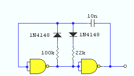
5. Pulse Reading Logic Probe
Note:
This logic probe uses a single CMOS IC and shows three logic conditions, High, Low and Pulsing. In addition if the probe input is neither hi or low (the high impedance state of tri-output logic ic's) then no LED's will light. Power from the logic probe is taken from the logic circuit under test; using a CMOS IC enables logic circuits to be tested using voltages from 3 to 15 volts. IC1a is arranged as a buffer with a difference. Under no input, i.e. probe not connected to circuit the gate will oscillate due to feedback from the 2M2 resistor. Output voltage at IC1a is approximately half supply voltage. The Hi and Lo logic indicator LED's are also connected to a potential divider consisting of the two 1k resistors. Voltage at the junction is half supply voltage hence with no input , or high impedance no LED's will light. A Hi or Lo logic condition will cause IC1a to rest in a permanent state indicated by either the Hi or Lo LED illuminating. With a fast oscillator or clock signal both Hi and Lo LED's will light but will be quite dim. This is the reason for IC1b and IC1c. These two gates form a monostable oscillator, time constant determined by the 100n capacitor and 4M7 resistor. With a clock signal this is effectively slowed as the monostable is continually triggered and retriggered. IC1d acts as a buffer to drive the pulsing LED.

Notes:
Built around a single 8038 waveform generator IC, this circuit produces sine, square or triangle waves from 20Hz to 200kHz in four switched ranges. There are both high and low level outputs which may be adjusted with the level control. This project makes a useful addition to any hobbyists workbench as well.
All of the waveform generation is produced by IC1. This versatile IC even has a sweep input, but is not used in this circuit. The IC contains an internal squarewave oscillator, the frequency of which is controlled by timing capacitors C1 - C4 and the 10k potentiometer. The tolerance of the capacitors should be 10% or better for stability. The squarewave is differentiated to produce a triangular wave, which in turn is shaped to produce a sine wave. All this is done internally, with a minimum of external components. The purity of the sine wave is adjusted by the two 100k preset resistors.
The wave shape switch is a single pole 3 way rotary switch, the wiper arm selects the wave shape and is connected to a 10k potentiometer which controls the amplitude of all waveforms. IC2 is an LF351 op-amp wired as a standard direct coupled non-inverting buffer, providing isolation between the waveform generator, and also increasing output current. The 2.2k and 47 ohm resistors form the output attenuator. At the high output, the maximum amplitude is about 8V pk-pk with the square wave. The maximum for the triangle and sine waves is around 6V and 4V respectively. The low amplitude controls is useful for testing amplifiers, as amplitudes of 20mV and 50mV are easily achievable.
Setting Up:
The two 100k preset resistors adjust the purity of the sine wave. If adjusted correctly, then the distortion amounts to less than 1%. The output waveform ideally needs to be monitored with an oscilloscope, but most people reading this will not have access to one. There is however, an easy alternative:- Winscope. This piece of software uses your soundcard and turns your computer into an oscilloscope. It even has storage facility and a spectrum analyser, however it will only work up to around 20KHz or so. Needless to say, this is more than adequate for this circuit, as alignment on any range automatically aligns other ranges as well. Winscope is available on the following page click here. Winscope is freeware and designed by Konstantin Zeldovich. After downloading, read the manual supplied with winscope and make up a lead to your soundcard. My soundcard is a SoundBlaster with a stereo line input, i made up a lead with both left and right inputs connected together. Connect the lead to the high output of the function generator, set the output level to high, shape to sine, and use the 1k to 10k range, (22nF capacitor). A waveform should be displayed, see the Figure 1 below:-
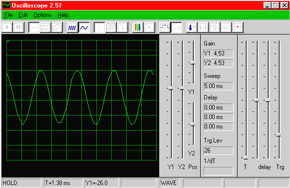
Figure 1.
Here an undistorted sine wave is being displayed. The display on winscope may flicker, this is normal as it uses your soundcard to take samples of the input waveform. The "hold" button on winscope will display a steady waveform.
Alignment:
First adjust the 100k preset connected to Pin 1 of the 8038. An incorrect setting will look similar to the waveform below:-
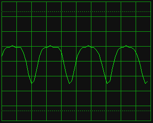
Adjust the preset so that the top of the sine wave has a nicely rounded peak. Then adjust the other preset, again an incorrectly adjusted waveform is shown below:

The two presets work together, so adjusting one affects the other. A little is all that's needed. When your waveform is adjusted and looks similar to Figure 1 press the FFT button on winscope. This will perform a fast Fourier transform and the displayed output will be a spectrogram of the input. For a pure sine wave, only one signal is present, the fundamental frequency, no harmonics will be present and so a spectrogram for a pure sine should contain a single spike, see Figure 2 below:-
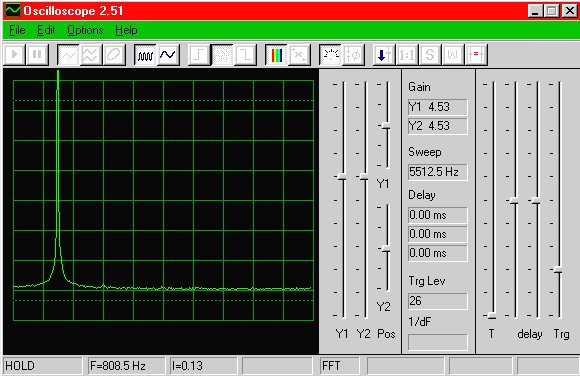
Figure 2.
A distorted sine wave will contain odd and even harmonics, and although the shape of the sine may look good, the spectrogram will reveal spikes at the harmonics, see below:-

Once alignment of the sine wave is complete, the other wave shapes will also be set up correctly. Below is a picture of the triangle waveform generated from my circuit:-

7. Multiwire Cable Tester
Description:
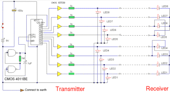
A multi wire cable tester with a separate LED for each wire. Will show open circuits, short circuits, reversals, earth faults, continuity and all with four IC's. Designed initially for my intercom, but can be used with alarm wiring, CAT 5 cables and more.
IC Pinouts of the 4011 and 4017 can also be viewed here
Circuit Notes:
Please note that for clarity this circuit has been drawn without showing power supplies to the CMOS 4011 and CMOS 4050 IC's. The positive battery terminal connects to Pin 14 of each IC and negative to Pin 7. The CMOS 4017 uses Pin 16 and Pin 8 respectively. Note also that as the CMOS 4050 is only a hex buffer, you need 8 gates so two 4050's are required, the unused inputs are connected to ground (battery negative terminal).
Circuit Description:
The circuit comprises transmitter and receiver, the cable under test linking the two. The transmitter is nothing more than a "LED chaser" the 4011 IC is wired as astable and clocks a 4017 decade counter divider. The 4017 is arranged so that on the 9th pulse, the count is reset. Each LED will light sequentially from LED 1 to LED 8 then back to LED 1 etc. As the 4017 has limited driving capabilities, then each output is buffered by a 4050. This provides sufficient current boost for long cables and the transmitter and receiver LED's. The receiver is simply 8 LED's with a common wire...read on.
Wiring the CMOS 4017
The pinout for the CMOS 4017B is shown below. Please note that in the main schematic above, alternate naming of the pins has been used. The pin equivalence is as follows:-
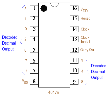
CP0 (clock pulse zero) is the Clock input, Pin 14 on the diagram above.
CP1 (clock pulse one) is the clock inhibit or Pin 13 on the pinout above.
MR (master reset) is the reset pin 15 in the diagram above.
Q0-9 represent the decoded decimal outputs. Hence Q0 is Pin 3 on the pinout and Q8 is Pin9.
7 Led's 8 Wires:
Not a mistype. The problem with testing each wire individually is that if you had 7 individually addressable LED's, then you would need an eighth return or common wire. In the case of testing 8 wires you would need a ninth wire. You could use a domestic earth but its not really practical, and also if the cable was shorting to earth anyway it would be no good anyway. The solution had me thinking for a while, but since this is a logic circuit, there are only two conditions, logic high or zero. As the 4017 outputs are either high or low, any output can provide a common return path for a LED. So LED's 1 - 3 use the 4th output of the 4017, which will be zero, and the 4th LED is wired with reverse polarity. On the 4th pulse, output 4 is high, output 3 is low and so the LED will light. If the common return wire is open circuit then LEDs 1-4 will not light. A similar situation occurs with outputs 5 to 8. The common wire in can be taken from any output terminal from the 4017, but the same rule would still apply. The ability to test all wires quickly outweighs this small disadvantage. If a cable of just 4 or 6 wires is tested then it must use the wires with LED's numbered 1 to 4 or 1 to 6, which is why the LED's are numbered that way.
Testing:
With a good cable and all wires connected then LED 1 will light at both cable ends, followed in sequence by LED 2 ,3, 4 etc to LED 8, the sequence then repeating. If a 4 wire cable is used, it must be connected to use the common return wire as described in the preceding paragraph. The sequence would be LED 1,2,3,4 repeating with a delay as the 4 unused outputs are stepped through.
To check for earth contact faults, the probe labeled "to earth connection" would be physically connected to a local earth. A wire that is earthing will dim or extinguish the LED's at both ends of the cable. An LED not lighting at the receiver, indicates a broken or open circuit. If two wires are short circuit, example 3 and 4 then at the receiver the sequence would be 1, 2, 34, 43, 5, 6, 7, 8. A reversal would be indicated by an out of pattern sequence of LED's. Here's an example, the probe is connected to an earth at the transmitter, the cable is very faulty, wire 1 is OK, 2 is earthing, 3 and 5 are reversed 4 is OK, 6 is open circuit and 7 and 8 are short circuit. See below.
Test Result for Above Faulty Cable:
The transmitter pattern: The receiver pattern would be:
1 ON 1 ON
2 OFF or Faint 2 OFF or faint
3 ON 3 (would show LED 5)
4 ON 4 ON
5 ON 5 (would show LED 3)
6 ON 6 OFF
7 ON 7 (would show 7 & 8)
8 ON 8 (would show 7 & 8)
The LED sequence of course is stepped through, as you know the transmitter "pattern" it is easy to tell the state of the cable by viewing the receiver pattern. The earth condition will only show up if the contact to earth is less than 1000 ohms, a better but more time consuming method foe earth faults is to use a meter on the Mega ohms range.
A low resistance ( 0.25 - 4 ohm) continuity tester for checking soldered joints and connections.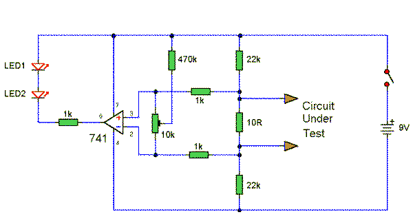
Notes:
This simple circuit uses a 741 op-amp in differential mode as a continuity tester. The voltage difference between the non-inverting and inverting inputs is amplified by the full open loop gain of the op-amp. Ignore the 470k and the 10k control for the moment, and look at the input of the op-amp. If the resistors were perfectly matched, then the voltage difference would be zero and output zero. However the use of the 470k and 10k control allows a small potential difference to be applied across the op-amp inputs and upset the balance of the circuit. This is amplified causing the op-amp output to swing to full supply voltage and light the LED's.
Setting Up and Testing:
The probes should first be connected to a resistor of value between 0.22 ohm and 4ohm. The control is adjusted until the LED's just light with the resistance across the probes. The resistor should then be removed and probes short circuited, the LED's should go out. As the low resistance value is extremely low, it is important that the probes, (whether crocodile clips or needles etc) be kept clean, otherwise dirt can increase contact resistance and cause the circuit to mis-operate. The circuit should also work with a MOSFET type op-amp such as CA3130, CA3140, and JFET types, e.g. LF351. If the lED's will not extinguish then a 10k preset should be wired across the offset null terminals, pins 1 and 5, the wiper of the control being connected to the negative battery terminal. A pin out for the 741 can also be found here
A classic Wien Bridge oscillator using an Op-Amp covering a frequency range of 15 to 150kHz in four switched steps.
Notes:
Two conditions exist for a sinusoidal oscillator. Regenerative or positive feedback, and a closed loop gain of unity. The losses in the wien feedback circuit, are such that the open loop gain of the amplifier must also exceed 29. The following link also provides the wien oscillator theory:
Wien Oscillator Theory
In this circuit the gain is provided by a FET type op-amp. I have used an LF351, which may be hard to obtain, but the TL071CN or TL081CN may be used and have a faster slewing rate than the LF351. The Maplin order codes are RA67X and RA70M respectively. The wien network is a parallel combination of resistor and capacitor, in series with a serial R-C network. Regenerative feedback is applied from the op-amp output, to the serial R-C input and continues. Stabilization is required to prevent the otherwise uncontrolled oscillation from building up and becoming unstable.
Stability and Distortion
There are two common methods of stabilizing a wien type oscillator. A thermistor with a NTC in the series leg of the feedback loop or an incandescent lamp (with a positive temperature coefficient) in the shunt leg of the feedback loop. The bulb used here is a 6V 60mA type Maplin code BT99H. A 12 Volt bulb rated 60mA or 40mA will also work. The feedback arrangement works as follows. As a bulb heats up its filament resistance increases. This will decrease the overall gain of the amplifier, as the output signal is fed back to the input. Similarly, if the output amplitude decreased the signal appearing at the bulb would be less, its filament resistance would drop and gain would be increased. Therefore a stable output amplitude is produced. The 1k preset is adjusted for minimum distortion. Note that split supplies are used and a ganged 10k potentiometer controls frequency with a 10:1 range.
Two simple test circuits to check operation of quartz crystals.

Notes:
In the first circuit, above the BC548 is wired as a colpitts oscillator, the frequency tuned by insertion of a crystal. A good crystal will create high frequency oscillations, the output at the collector is rectified by the germanium OA91 diode and a deflection will appear on the meter. The more active the crystal, the higher the output deflection which may be adjusted with the preset.

Notes:
The next circuit uses a working crystal again used to control the frequency of a colpitts oscillator. This time the output from the oscillator is taken from the emitter and is full wave rectified, the small dc bias will then directly cause the second BC548 to light the LED.
A simple test circuit to fault find audio and radio equipment. Can be used to inject a square wave signal, rich in harmonics, or used with headphones as an audio tracer.
 Notes:
A single pole double throw switch is used to switch between inject and trace modes. The diagram is drawn in trace mode, the earpiece being connected to the collector of the last transistor. Both transistors are wired as emitter followers, providing high gain. DC blocking is provided by the 1n capacitor at the probe end, and the two stages are capacitive coupled.
when the switch is thrown the opposite way (to the blue dot) both transistors are wired as an astable square wave generator. This provides enough harmonics from audio up to several hundred kilohertz and is useful for testing AM radio Receivers.
A Beat Balance Metal Detector made from discrete components.

Notes:
Various embodiments of the BB metal detector have been published, and it has been widely described in the press as a new genre. Instead of using a search and a reference oscillator as with BFO, or Tx and Rx coils as with IB, it uses two transmitters or search oscillators with IB-style coil overlap. The frequencies of the two oscillators are then mixed in similar fashion to BFO, to produce an audible heterodyne. On the surface of it, this design would seem to represent little more than a twinned BFO metal detector. However, what makes it different above all else, and significantly increases its range, is that each coil modifies the frequency of the adjacent oscillator through mutual coupling. This introduces the "balance" that is present in an IB metal detector, and boosts sensitivity well beyond that of BFO. Since the concept borrows from both BFO and IB, I have given a nod to each of these by naming it a Beat Balance Metal Detector, or BB for short. Happy hunting!
A Coil Coupled Operation Metal Detector made from readily obtainable components and using an ordinary medium receiver as a detector.

Notes:
The metal detector shown here may well represent a new genre. At any rate, after some exposure, it is regarded as such by those who have seen it. It is based on a standard transformer coupled oscillator (TCO) - hence the name Coil Coupled Operation (CCO) Metal Detector. Although requiring a BFO (in this case provided by a Medium Wave radio), it differs from a typical BFO detector in that its performance far outstrips that of BFO. Also, unlike BFO, it is dependent on the balance of two coils to boost sensitivity. It also differs from IB, in that its Rx section is an active, rather than passive, component of the oscillator. Further, unlike IB, the design does not require critical placement of the coils. As with both BFO and IB, the design provides discrimination. Experiments with different embodiments of the idea have shown that it has the potential to match the best of IB. Happy hunting.
A small 325mW amplifier with a voltage gain of 200 that can be used as a bench amplifier, signal tracer or used to amplify the output from personal radios, etc.
Notes:
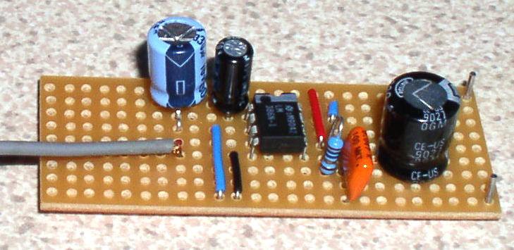
The circuit is based on the National Semiconductor LM386 amplifier. In the diagram above, the LM386 forms a complete non-inverting amplifier with voltage gain of x200.
A datasheet in PDF format can be downloaded from the National Semiconductor website. The IC is available in an 8 pin DIL package and several versions are available; the LM386N-1 which has 325mW output into an 8 ohm load, the Lm386N-3 which has 700mW output and the LM386N-4 which offers 1000mW output. all versions work in this circuit.
The gain of the Lm386 can be controlled by the capacitor across pins 1 and 8. With the 10u cap shown above, voltage gain is 200, omitting this capacitor and the gain of the amplifier is 20.
The IC works from 4 to 12Volts DC, 12Volt being the maximum recommended value. The internal input impedance of the amplifier is 50K, this is shunted with a 22k log potentiometer so input impedance in this circuit will be lower at about 15k. The input is DC coupled so care must be taken not to amplify any DC from the preceding circuit, otherwise the loudspeaker may be damaged. A coupling capacitor may included in series with the 22k control to prevent this from happening.
The finished circuit.
This logic probe uses a single CMOS IC and shows three logic conditions, High, Low and Pulsing. In addition if the probe input is neither hi or low (the high impedance state of tri-output logic ic's) then no LED's will light. Power from the logic probe is taken from the logic circuit under test; using a CMOS IC enables logic circuits to be tested using voltages from 3 to 15 volts. IC1a is arranged as a buffer with a difference. Under no input, i.e. probe not connected to circuit the gate will oscillate due to feedback from the 2M2 resistor. Output voltage at IC1a is approximately half supply voltage. The Hi and Lo logic indicator LED's are also connected to a potential divider consisting of the two 1k resistors. Voltage at the junction is half supply voltage hence with no input , or high impedance no LED's will light. A Hi or Lo logic condition will cause IC1a to rest in a permanent state indicated by either the Hi or Lo LED illuminating. With a fast oscillator or clock signal both Hi and Lo LED's will light but will be quite dim. This is the reason for IC1b and IC1c. These two gates form a monostable oscillator, time constant determined by the 100n capacitor and 4M7 resistor. With a clock signal this is effectively slowed as the monostable is continually triggered and retriggered. IC1d acts as a buffer to drive the pulsing LED.
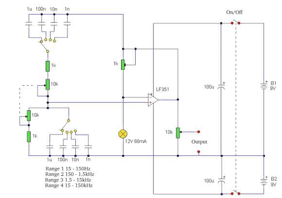
6. Function Generator
Built around a single 8038 waveform generator IC, this circuit produces sine, square or triangle waves from 20Hz to 200kHz in four switched ranges. There are both high and low level outputs which may be adjusted with the level control. This project makes a useful addition to any hobbyists workbench as well.
All of the waveform generation is produced by IC1. This versatile IC even has a sweep input, but is not used in this circuit. The IC contains an internal squarewave oscillator, the frequency of which is controlled by timing capacitors C1 - C4 and the 10k potentiometer. The tolerance of the capacitors should be 10% or better for stability. The squarewave is differentiated to produce a triangular wave, which in turn is shaped to produce a sine wave. All this is done internally, with a minimum of external components. The purity of the sine wave is adjusted by the two 100k preset resistors.
The wave shape switch is a single pole 3 way rotary switch, the wiper arm selects the wave shape and is connected to a 10k potentiometer which controls the amplitude of all waveforms. IC2 is an LF351 op-amp wired as a standard direct coupled non-inverting buffer, providing isolation between the waveform generator, and also increasing output current. The 2.2k and 47 ohm resistors form the output attenuator. At the high output, the maximum amplitude is about 8V pk-pk with the square wave. The maximum for the triangle and sine waves is around 6V and 4V respectively. The low amplitude controls is useful for testing amplifiers, as amplitudes of 20mV and 50mV are easily achievable.
Setting Up:
The two 100k preset resistors adjust the purity of the sine wave. If adjusted correctly, then the distortion amounts to less than 1%. The output waveform ideally needs to be monitored with an oscilloscope, but most people reading this will not have access to one. There is however, an easy alternative:- Winscope. This piece of software uses your soundcard and turns your computer into an oscilloscope. It even has storage facility and a spectrum analyser, however it will only work up to around 20KHz or so. Needless to say, this is more than adequate for this circuit, as alignment on any range automatically aligns other ranges as well. Winscope is available on the following page click here. Winscope is freeware and designed by Konstantin Zeldovich. After downloading, read the manual supplied with winscope and make up a lead to your soundcard. My soundcard is a SoundBlaster with a stereo line input, i made up a lead with both left and right inputs connected together. Connect the lead to the high output of the function generator, set the output level to high, shape to sine, and use the 1k to 10k range, (22nF capacitor). A waveform should be displayed, see the Figure 1 below:-
Figure 1.
Here an undistorted sine wave is being displayed. The display on winscope may flicker, this is normal as it uses your soundcard to take samples of the input waveform. The "hold" button on winscope will display a steady waveform.
Alignment:
First adjust the 100k preset connected to Pin 1 of the 8038. An incorrect setting will look similar to the waveform below:-
Adjust the preset so that the top of the sine wave has a nicely rounded peak. Then adjust the other preset, again an incorrectly adjusted waveform is shown below:
The two presets work together, so adjusting one affects the other. A little is all that's needed. When your waveform is adjusted and looks similar to Figure 1 press the FFT button on winscope. This will perform a fast Fourier transform and the displayed output will be a spectrogram of the input. For a pure sine wave, only one signal is present, the fundamental frequency, no harmonics will be present and so a spectrogram for a pure sine should contain a single spike, see Figure 2 below:-
Figure 2.
A distorted sine wave will contain odd and even harmonics, and although the shape of the sine may look good, the spectrogram will reveal spikes at the harmonics, see below:-
Once alignment of the sine wave is complete, the other wave shapes will also be set up correctly. Below is a picture of the triangle waveform generated from my circuit:-
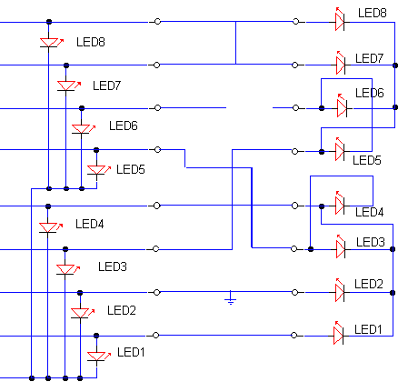
7. Multiwire Cable Tester
Description:
A multi wire cable tester with a separate LED for each wire. Will show open circuits, short circuits, reversals, earth faults, continuity and all with four IC's. Designed initially for my intercom, but can be used with alarm wiring, CAT 5 cables and more.
IC Pinouts of the 4011 and 4017 can also be viewed here
Circuit Notes:
Please note that for clarity this circuit has been drawn without showing power supplies to the CMOS 4011 and CMOS 4050 IC's. The positive battery terminal connects to Pin 14 of each IC and negative to Pin 7. The CMOS 4017 uses Pin 16 and Pin 8 respectively. Note also that as the CMOS 4050 is only a hex buffer, you need 8 gates so two 4050's are required, the unused inputs are connected to ground (battery negative terminal).
Circuit Description:
The circuit comprises transmitter and receiver, the cable under test linking the two. The transmitter is nothing more than a "LED chaser" the 4011 IC is wired as astable and clocks a 4017 decade counter divider. The 4017 is arranged so that on the 9th pulse, the count is reset. Each LED will light sequentially from LED 1 to LED 8 then back to LED 1 etc. As the 4017 has limited driving capabilities, then each output is buffered by a 4050. This provides sufficient current boost for long cables and the transmitter and receiver LED's. The receiver is simply 8 LED's with a common wire...read on.
Wiring the CMOS 4017
The pinout for the CMOS 4017B is shown below. Please note that in the main schematic above, alternate naming of the pins has been used. The pin equivalence is as follows:-
CP0 (clock pulse zero) is the Clock input, Pin 14 on the diagram above.
CP1 (clock pulse one) is the clock inhibit or Pin 13 on the pinout above.
MR (master reset) is the reset pin 15 in the diagram above.
Q0-9 represent the decoded decimal outputs. Hence Q0 is Pin 3 on the pinout and Q8 is Pin9.
7 Led's 8 Wires:
Not a mistype. The problem with testing each wire individually is that if you had 7 individually addressable LED's, then you would need an eighth return or common wire. In the case of testing 8 wires you would need a ninth wire. You could use a domestic earth but its not really practical, and also if the cable was shorting to earth anyway it would be no good anyway. The solution had me thinking for a while, but since this is a logic circuit, there are only two conditions, logic high or zero. As the 4017 outputs are either high or low, any output can provide a common return path for a LED. So LED's 1 - 3 use the 4th output of the 4017, which will be zero, and the 4th LED is wired with reverse polarity. On the 4th pulse, output 4 is high, output 3 is low and so the LED will light. If the common return wire is open circuit then LEDs 1-4 will not light. A similar situation occurs with outputs 5 to 8. The common wire in can be taken from any output terminal from the 4017, but the same rule would still apply. The ability to test all wires quickly outweighs this small disadvantage. If a cable of just 4 or 6 wires is tested then it must use the wires with LED's numbered 1 to 4 or 1 to 6, which is why the LED's are numbered that way.
Testing:
With a good cable and all wires connected then LED 1 will light at both cable ends, followed in sequence by LED 2 ,3, 4 etc to LED 8, the sequence then repeating. If a 4 wire cable is used, it must be connected to use the common return wire as described in the preceding paragraph. The sequence would be LED 1,2,3,4 repeating with a delay as the 4 unused outputs are stepped through.
To check for earth contact faults, the probe labeled "to earth connection" would be physically connected to a local earth. A wire that is earthing will dim or extinguish the LED's at both ends of the cable. An LED not lighting at the receiver, indicates a broken or open circuit. If two wires are short circuit, example 3 and 4 then at the receiver the sequence would be 1, 2, 34, 43, 5, 6, 7, 8. A reversal would be indicated by an out of pattern sequence of LED's. Here's an example, the probe is connected to an earth at the transmitter, the cable is very faulty, wire 1 is OK, 2 is earthing, 3 and 5 are reversed 4 is OK, 6 is open circuit and 7 and 8 are short circuit. See below.
Test Result for Above Faulty Cable:
The transmitter pattern: The receiver pattern would be:
1 ON 1 ON
2 OFF or Faint 2 OFF or faint
3 ON 3 (would show LED 5)
4 ON 4 ON
5 ON 5 (would show LED 3)
6 ON 6 OFF
7 ON 7 (would show 7 & 8)
8 ON 8 (would show 7 & 8)
The LED sequence of course is stepped through, as you know the transmitter "pattern" it is easy to tell the state of the cable by viewing the receiver pattern. The earth condition will only show up if the contact to earth is less than 1000 ohms, a better but more time consuming method foe earth faults is to use a meter on the Mega ohms range.
8. Connection Tester
Description:A low resistance ( 0.25 - 4 ohm) continuity tester for checking soldered joints and connections.
Notes:
This simple circuit uses a 741 op-amp in differential mode as a continuity tester. The voltage difference between the non-inverting and inverting inputs is amplified by the full open loop gain of the op-amp. Ignore the 470k and the 10k control for the moment, and look at the input of the op-amp. If the resistors were perfectly matched, then the voltage difference would be zero and output zero. However the use of the 470k and 10k control allows a small potential difference to be applied across the op-amp inputs and upset the balance of the circuit. This is amplified causing the op-amp output to swing to full supply voltage and light the LED's.
Setting Up and Testing:
The probes should first be connected to a resistor of value between 0.22 ohm and 4ohm. The control is adjusted until the LED's just light with the resistance across the probes. The resistor should then be removed and probes short circuited, the LED's should go out. As the low resistance value is extremely low, it is important that the probes, (whether crocodile clips or needles etc) be kept clean, otherwise dirt can increase contact resistance and cause the circuit to mis-operate. The circuit should also work with a MOSFET type op-amp such as CA3130, CA3140, and JFET types, e.g. LF351. If the lED's will not extinguish then a 10k preset should be wired across the offset null terminals, pins 1 and 5, the wiper of the control being connected to the negative battery terminal. A pin out for the 741 can also be found here
9. Sinewave Generator
Description:A classic Wien Bridge oscillator using an Op-Amp covering a frequency range of 15 to 150kHz in four switched steps.
Notes:
Two conditions exist for a sinusoidal oscillator. Regenerative or positive feedback, and a closed loop gain of unity. The losses in the wien feedback circuit, are such that the open loop gain of the amplifier must also exceed 29. The following link also provides the wien oscillator theory:
Wien Oscillator Theory
In this circuit the gain is provided by a FET type op-amp. I have used an LF351, which may be hard to obtain, but the TL071CN or TL081CN may be used and have a faster slewing rate than the LF351. The Maplin order codes are RA67X and RA70M respectively. The wien network is a parallel combination of resistor and capacitor, in series with a serial R-C network. Regenerative feedback is applied from the op-amp output, to the serial R-C input and continues. Stabilization is required to prevent the otherwise uncontrolled oscillation from building up and becoming unstable.
Stability and Distortion
There are two common methods of stabilizing a wien type oscillator. A thermistor with a NTC in the series leg of the feedback loop or an incandescent lamp (with a positive temperature coefficient) in the shunt leg of the feedback loop. The bulb used here is a 6V 60mA type Maplin code BT99H. A 12 Volt bulb rated 60mA or 40mA will also work. The feedback arrangement works as follows. As a bulb heats up its filament resistance increases. This will decrease the overall gain of the amplifier, as the output signal is fed back to the input. Similarly, if the output amplitude decreased the signal appearing at the bulb would be less, its filament resistance would drop and gain would be increased. Therefore a stable output amplitude is produced. The 1k preset is adjusted for minimum distortion. Note that split supplies are used and a ganged 10k potentiometer controls frequency with a 10:1 range.
10. Two Crystal Test Circuits
Description:Two simple test circuits to check operation of quartz crystals.
Notes:
In the first circuit, above the BC548 is wired as a colpitts oscillator, the frequency tuned by insertion of a crystal. A good crystal will create high frequency oscillations, the output at the collector is rectified by the germanium OA91 diode and a deflection will appear on the meter. The more active the crystal, the higher the output deflection which may be adjusted with the preset.
Notes:
The next circuit uses a working crystal again used to control the frequency of a colpitts oscillator. This time the output from the oscillator is taken from the emitter and is full wave rectified, the small dc bias will then directly cause the second BC548 to light the LED.
11. Signal Injector and Tracer
Description:A simple test circuit to fault find audio and radio equipment. Can be used to inject a square wave signal, rich in harmonics, or used with headphones as an audio tracer.
A single pole double throw switch is used to switch between inject and trace modes. The diagram is drawn in trace mode, the earpiece being connected to the collector of the last transistor. Both transistors are wired as emitter followers, providing high gain. DC blocking is provided by the 1n capacitor at the probe end, and the two stages are capacitive coupled.
when the switch is thrown the opposite way (to the blue dot) both transistors are wired as an astable square wave generator. This provides enough harmonics from audio up to several hundred kilohertz and is useful for testing AM radio Receivers.
12. Beat Balance Metal Detector
Description:A Beat Balance Metal Detector made from discrete components.
Notes:
Various embodiments of the BB metal detector have been published, and it has been widely described in the press as a new genre. Instead of using a search and a reference oscillator as with BFO, or Tx and Rx coils as with IB, it uses two transmitters or search oscillators with IB-style coil overlap. The frequencies of the two oscillators are then mixed in similar fashion to BFO, to produce an audible heterodyne. On the surface of it, this design would seem to represent little more than a twinned BFO metal detector. However, what makes it different above all else, and significantly increases its range, is that each coil modifies the frequency of the adjacent oscillator through mutual coupling. This introduces the "balance" that is present in an IB metal detector, and boosts sensitivity well beyond that of BFO. Since the concept borrows from both BFO and IB, I have given a nod to each of these by naming it a Beat Balance Metal Detector, or BB for short. Happy hunting!
13. Coil Coupled Operation Metal Detector
Description:A Coil Coupled Operation Metal Detector made from readily obtainable components and using an ordinary medium receiver as a detector.
Notes:
The metal detector shown here may well represent a new genre. At any rate, after some exposure, it is regarded as such by those who have seen it. It is based on a standard transformer coupled oscillator (TCO) - hence the name Coil Coupled Operation (CCO) Metal Detector. Although requiring a BFO (in this case provided by a Medium Wave radio), it differs from a typical BFO detector in that its performance far outstrips that of BFO. Also, unlike BFO, it is dependent on the balance of two coils to boost sensitivity. It also differs from IB, in that its Rx section is an active, rather than passive, component of the oscillator. Further, unlike IB, the design does not require critical placement of the coils. As with both BFO and IB, the design provides discrimination. Experiments with different embodiments of the idea have shown that it has the potential to match the best of IB. Happy hunting.
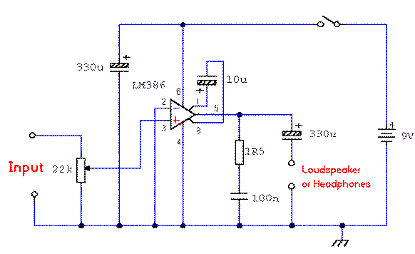
14. Bench Amplifier Circuit
Description:A small 325mW amplifier with a voltage gain of 200 that can be used as a bench amplifier, signal tracer or used to amplify the output from personal radios, etc.
Notes:
The circuit is based on the National Semiconductor LM386 amplifier. In the diagram above, the LM386 forms a complete non-inverting amplifier with voltage gain of x200.
A datasheet in PDF format can be downloaded from the National Semiconductor website. The IC is available in an 8 pin DIL package and several versions are available; the LM386N-1 which has 325mW output into an 8 ohm load, the Lm386N-3 which has 700mW output and the LM386N-4 which offers 1000mW output. all versions work in this circuit.
The gain of the Lm386 can be controlled by the capacitor across pins 1 and 8. With the 10u cap shown above, voltage gain is 200, omitting this capacitor and the gain of the amplifier is 20.
The IC works from 4 to 12Volts DC, 12Volt being the maximum recommended value. The internal input impedance of the amplifier is 50K, this is shunted with a 22k log potentiometer so input impedance in this circuit will be lower at about 15k. The input is DC coupled so care must be taken not to amplify any DC from the preceding circuit, otherwise the loudspeaker may be damaged. A coupling capacitor may included in series with the 22k control to prevent this from happening.
The finished circuit.
No comments:
Post a Comment